Can Mechanical Movements on FI‑CDM Tester Cause Additional Zap During CDM Stress?

This investigation is the first to examine how mechanical movements impact CDM stress, revealing that such movements add stress to the Device Under Test—a finding relevant for Field‑Induced CDM testers and any tester requiring part movement to trigger a zap. The study provided clear evidence of unwanted zaps caused by contact bouncing and proposed mitigation solutions. Based on these findings, the tester supplier modified the tester’s software, representing evolutionary but significant progress in improving test accuracy and reliability.
During FI-CDM testing, discharge current polarity can sometimes oppose the stress condition. In Figure 1, a negative zap occurs despite a +500V stress condition. We refer to this unintended zap as a secondary discharge.
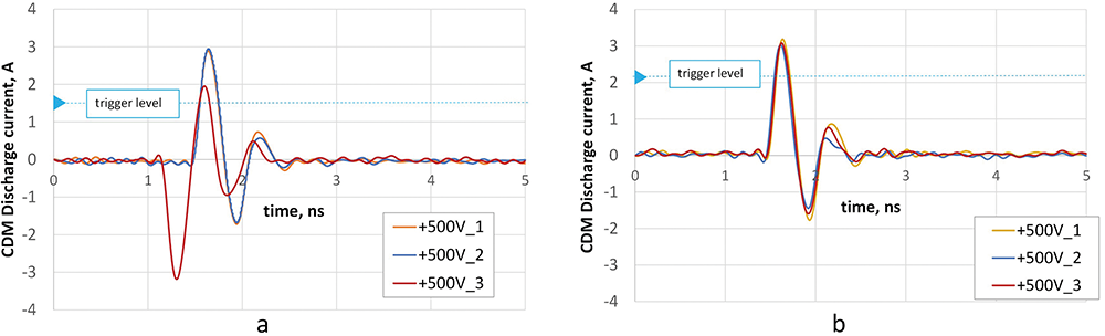 Figure 1: CDM waveform data at TC+500V on H8 with different trigger levels.
Secondary discharges occur inconsistently and only in certain package types, specifically in Single Discharge mode.
During CDM stress, the test part is placed in a dead‑bug position on a field plate. A CDM discharge is triggered when the pogo pin contacts the part [1]. Both the discharge head and pogo pin are grounded. The discharge head’s movement is motor-controlled, guided by software and the x, y, z coordinates set during part alignment [2].
Is Secondary Discharge Possible in Theory?
Let’s examine the tester architecture and operation to determine if mechanical vibrations on the pogo pin can cause secondary discharge. Figure 2 illustrates the sequence of events during a single zap in SD mode.
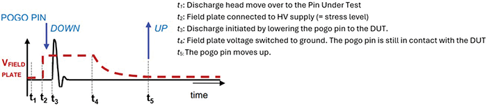 Figure 2: Single Discharge procedure (Annex H of JS-002)
Figure 3 explores the charge and voltage on the IC during the different steps mentioned above.
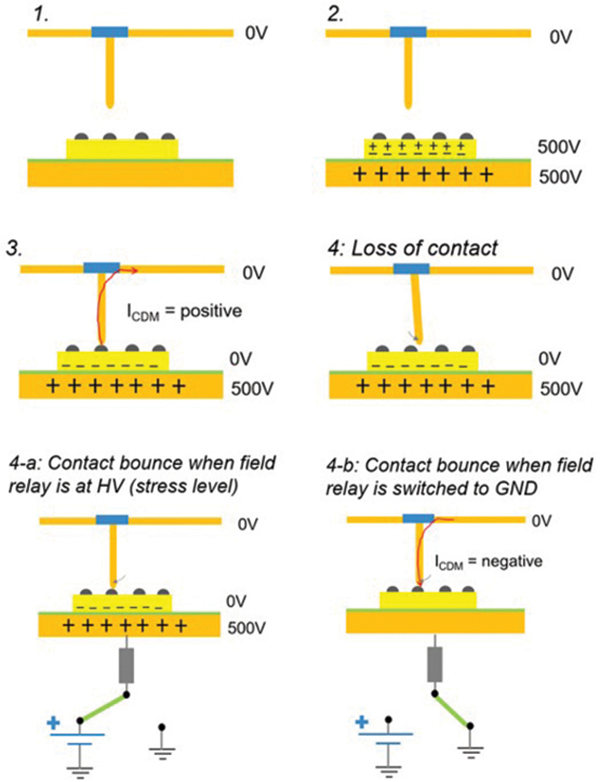 Figure 3: Charge and voltage values during a CDM event at TC+500 in SD mode
Steps 1 to 3 proceed as expected. However, if the pogo pin loses contact in the down position due to misalignment or mechanical bouncing (Step 4), a subsequent contact may trigger a secondary discharge. This occurs only if the field plate voltage differs from that at the previous contact in Figure 4.
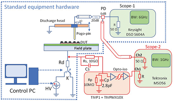 Figure 4: Measurement setup for simultaneous monitoring of CDM pulse and charge plate potential.
Proof of Secondary Discharge
Now that we have established its theoretical possibility, it must be validated through measurements. To study this event, we first need to make it reproducible. This was achieved by applying CDM stress to a verification coin, deliberately misaligning the pogo pin to touch its edge and ensure contact loss.
Measurement 1: Monitor field plate voltage and CDM discharge currents simultaneously
Figure 4 illustrates the measurement setup used for this study, with standard equipment hardware shown in blue and adaptations in red. A deep-memory oscilloscope (Scope-2) with a high sampling rate and 1 GHz bandwidth monitors both the CDM current and the field plate voltage simultaneously, as shown in Figure 5.
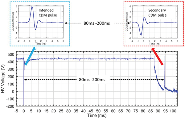 Figure 5: Graph showing field plate voltage and the corresponding CDM current, during a TC +500V
From the several measurements, we see the following:
- In the SD mode, secondary discharge occurs just after the voltage on field plate switches from HV to ground.
- The discharge time set in the test program does not have any impact on the duration of the HV on field plate nor the time at which the secondary discharge occurs.
Measurement 2: Electrical measurement of contact bouncing
Measurement set-up to make the breaking events visible by electrical measurements is shown in Figure 6. With this set-up, we expect Vsense to read 100mV in case of good contact of pogo pin with DUT and 0V when there is no contact.
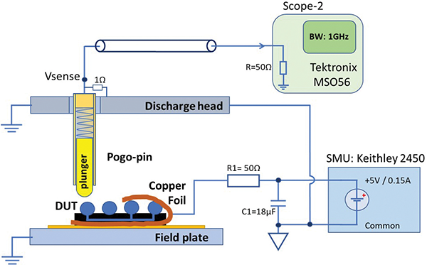 Figure 6: Measurement set-up for monitoring electrical contact between pogo and DUT.
Voltage measured at Vsense for several Z-stop settings is shown in Figure 7. Z-stop is the alignment position in the z-direction. Also marked in the graph are the timings of the relevant events. When z = Z-stop, the motor stops movement. The higher the magnitude of z, the deeper the pogo is pushed. From Figure 7d we see that when Z-stop = 100.96mm, there is no mechanical bouncing. But when Z-stop=100.83mm, the pogo pin does not make contact for most of the time. For any z in between, the contact is broken several times.
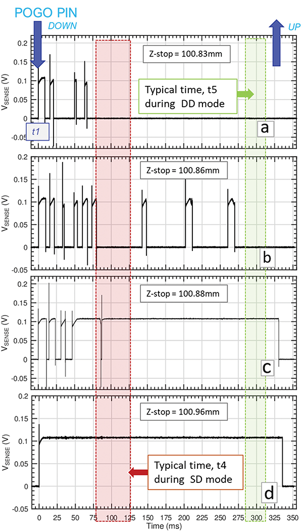 Figure 7: Ohmic contact between pogo-pin and DUT for several Z-stop values
Conclusion
Secondary discharge is observed when switching of the field plate voltage and mechanical bouncing occurs around the same time. Unfortunately, mechanical vibrations and misaligned pins cannot be totally avoided. To avoid secondary discharge:
- Increase the overdrive in z-direction. Be careful. Too much overdrive can push the sample away.
- Change tester firmware to ensure switching of the field plate voltage after the vibrations have damped out.
References
- ESDA/JEDEC JS-002-2022, “Charged Device Model (CDM) Device Level”, 2022.
- Orion 3 CDM Test System. Operation Manual MA-70-100-005-00-A Thermo Fisher Scientific, 2017.