On-Chip ESD Protection for Multi‑Gbps Automotive Applications

The increasing demand for advanced driver assistance systems (ADAS) in road vehicles is fueling the development of high-speed automotive serial links. ADAS features such as adaptive cruise control, lane-keeping assistance, and parking assistance rely heavily on cameras, sensors, and radar. To support high image resolution and video frame rates, state-of‑the-art automotive I/O may operate at data rates higher than 10 Gbps [1]. Automotive ICs are rated for system-level ESD robustness, rather than only component-level ESD, which makes ESD protection design for high-speed automotive I/O more challenging than for most other high-speed I/O. Specifically, in addition to component-level ESD qualification tests like human body model (HBM) and charged device model (CDM), many automotive products need to pass ISO-10605 qualification [2], which is a test standard for road vehicles based in part on the similar but more general IEC 61000-4-2 standard. Figure 1 shows an example of an 8kV discharge current waveform. The near-30-A peak current is well above the magnitude of the HBM and CDM.
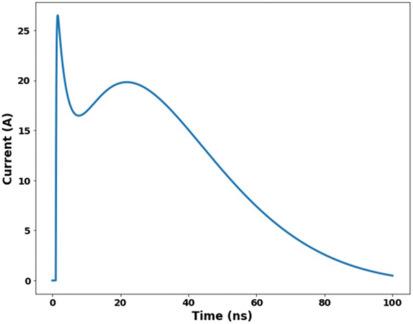 Figure 1: 8-kV ISO-10605 discharge current waveform into a low impedance load.
Conventionally, transient voltage suppressor (TVS) devices may be placed on a PC board to sink the system-level ESD current [3][4] as shown in Figure 2. While it is a widely adopted protection scheme for relatively low-speed interfaces such as the controller area network (CAN) bus, the impedance discontinuity introduced by the on-board TVS makes it challenging to meet both the ESD requirements and the performance specifications.
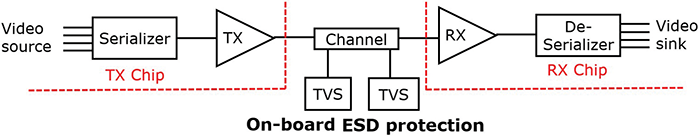 Figure 2: Illustration of the conventional on-board system-level ESD protection with TVS devices
One way to address the challenge is to place the ESD protection on-chip as shown in Figure 3, which allows the large ESD capacitance to be absorbed into a circuit network that will compensate for it. It is therefore highly desirable that the IC manufacturers of these receiver (RX) and transmitter (TX) chips integrate the ESD protection on-chip. System designers incorporating these chips into a complete system no longer need to worry about onboard ESD protection.
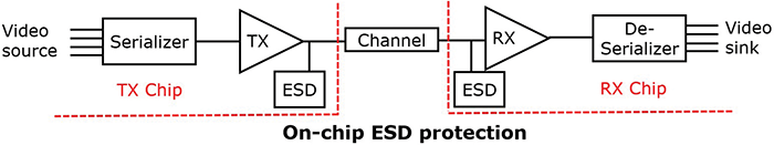 Figure 3: Illustration of the conventional on-chip system-level ESD protection
Figure 4 shows the schematic of the ESD-protected receiver front-end reported in this work [5]. Primary and secondary ESD clamps are embedded in a T-coil circuit, which is commonly used in broadband I/O circuits for impedance-matching and bandwidth extension. The T-coil is composed of two coupled inductors. The primary ESD protection, an efficient bidirectional SCR [6], is used to sink most of the ESD current. It is connected to the center tap of the T-coil. The input port of the T-coil is connected to the I/O Bump, and the output port of the T-coil is connected to a 50-Ω on-die termination (RODT) resistor. An AC-coupling capacitor CAC provides a bridge between the ODT and the first stage of the receiver circuit (RX), typically a continuous time linear equalizer (CTLE). Secondary and auxiliary dual-diodes are placed at the ODT side and RX side of CAC, respectively. The secondary ESD protection utilizes the impedance of the T-coil to first reduce the stress seen at the ODT. The auxiliary ESD protection stage further reduces the stress seen at the RX as demonstrated in [5] and [7].
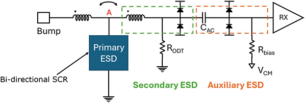 Figure 4: Schematic of the ESD-protection architecture of the receiver front-end
As reported in [5], the proposed on‑chip protection architecture can achieve up to 8kV ISO system-level protection. The measured and simulated return loss and insertion loss are plotted in Figures 5a and 5b, respectively. The return loss and insertion loss serve as good performance indicators of the ESD‑protected frontend network. The measured return loss remains below -13 dB, and the normalized insertion loss is less than 1 dB all the way to 18 GHz, indicating excellent impedance matching and bandwidth extension. The achieved bandwidth supports 36/72 Gbps data rates (NRZ/PAM4) and beyond, which is well above the data rate of today’s state-of-the-art automotive links.
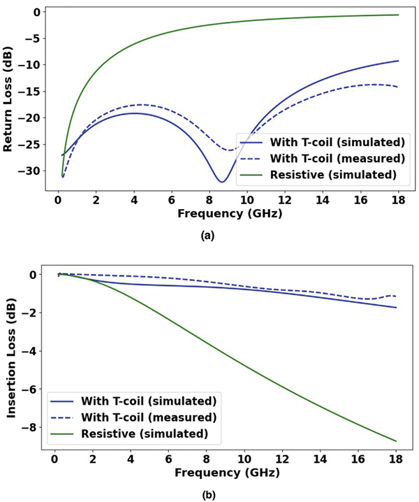 Figure 5: Measured and simulated (a) return loss and (b) insertion loss of the test structure.
In the future, automotive I/O will become faster with the integration of more ADAS features. Meeting the ESD robustness requirements of these systems will require careful co-design of system-level ESD protection and analog front-end circuits.
References
- “Gigabit Multimedia Serial Link (GMSL)” (accessed Feb. 1, 2025).
- Road Vehicles—Test Methods for Electrical Disturbances From Electrostatic Discharge, ISO Standard 10605, 2023.
- C.-H. Chuang and M.-D. Ker, “System-Level ESD Protection for Automotive Electronics by Co-Design of TVS and CAN Transceiver Chips,” IEEE Transactions on Device and Materials Reliability, vol. 17, no. 3, pp. 570-576, Sept. 2017
- Y. Xi, J.A. Salcedo, Y. Zhou, J. J. Liou, and J.-J. Hajjar, “Design and characterization of ESD solutions with EMC robustness for automotive applications”, Microelectronics Reliability, Vol. 55, No. 11, 2015
- S. Huang, S. Parthasarathy, Y.P. Zhou, J.-J. Hajjar, and E. Rosenbaum, “On-Chip ESD Protection for Multi-Gbps Automotive Serial IO in a 16-nm FinFET Process,” in 2024 46th Annual EOS/ESD Symposium (EOS/ESD), Reno, NV, USA, 2024, pp. 1-7
- S. Huang, S. Parthasarathy, Y.P. Zhou, J.-J. Hajjar, and E. Rosenbaum, “Poly-Bounded Silicon-Controlled-Rectifier for ESD Protection in FinFET Technology,” in 2023 International Electron Devices Meeting (IEDM), San Francisco, CA, USA, 2023, pp. 1-4
- S. Huang and E. Rosenbaum, “Optimized CDM-ESD Protection for 100+ Gbps Wireline IO in 16-nm CMOS,” in 2025 IEEE International Reliability Physics Symposium (IRPS), Monterey, CA, USA, 2025, pp. 1-9.