Part 1 An Introduction to ESD
- ESD Overview
- /
- ESD Fundamentals
- /
- Part 1: An Introduction to ESD
Fundamentals of Electrostatic Discharge
Part One—An Introduction to ESD
© 2020, EOS/ESD Association, Inc., Rome, NY
HISTORY & BACKGROUND
Greek scientist, Thales of Miletus mentioned the earliest report of electricity. He found that after amber was rubbed, dust and leaves were attracted to it. The word "triboelectric", covered later, comes from the Greek words, tribo – meaning "to rub" and elektros – meaning "amber" (fossilized resin from prehistoric trees). When flowing electricity properties were discovered in the 1700s, static electricity became the term for the old form of electricity, which distinguished it from the new forms of electricity.
Many people have experienced static electricity and "shocks", or electrostatic discharge (ESD) when touching a metal doorknob after walking across a carpeted floor or after sliding across a car seat. However, static electricity and ESD have created serious industrial problems for centuries. As early as the 1400s, European and Caribbean military forts were using static control procedures and grounding devices trying to prevent inadvertent ESD ignition of gunpowder stores. By the 1860s, paper mills throughout the
U.S. employed basic grounding, flame ionization techniques, and steam drums to dissipate static electricity from the paper web as it traveled through the drying process. Every imaginable business and industrial process has issues with an electrostatic charge and discharge at one time or another. Munitions and explosives, petrochemical, pharmaceutical, agriculture, printing and graphic arts, textiles, painting, and plastics are just some of the industries where control of static electricity has significant importance.
The age of electronics brought with it new problems associated with static electricity and ESD. And, as electronic devices become faster and the circuitry gets smaller, sensitivity to ESD in general increases. This trend may be accelerating. The EOS/ESD Association, Inc.'s Electrostatic Discharge (ESD) Technology Roadmap is revised every few years and states, "with devices becoming more sensitive, it is imperative that companies begin to scrutinize the ESD capabilities of their handling processes". Today, ESD impacts productivity and product reliability in virtually every aspect of the global electronics environment.
Despite a great deal of effort during the past decades, ESD still affects production yields, manufacturing cost, product quality, product reliability, and profitability. The cost of damaged devices ranges from only a few cents for a simple diode to thousands of dollars for complex integrated circuits. When associated costs of repair and rework, shipping, labor, and overhead are included, the opportunities exist for significant improvements. Nearly all of the thousands of companies involved in electronics manufacturing today pay attention to the basic industry-accepted elements of static control. EOS/ESD Association, Inc. industry standards are available today to guide manufacturers in establishing the fundamental static charge mitigation and control techniques (see Part Six – ESD
Standards). It is unlikely that any company which ignores static control will be able to manufacture and deliver undamaged electronic parts successfully.
STATIC ELECTRICITY: CREATING CHARGE
Definitions for ESD terminology can be found in ESD ADV1.0 - Glossary, which is available as a complimentary download at w ww.esda.org. Electrostatic charge is defined as "electric charge at rest". Static electricity is an imbalance of electrical charges within or on the surface of a material. This imbalance of electrons produces an electric field that can be measured and that can influence other objects. Electrostatic discharge (ESD) is defined as "the rapid, spontaneous transfer of electrostatic charge induced by a high electrostatic field. Note: Usually, the charge flows through a spark between two conductive bodies at different electrostatic potentials as they approach one another".
ESD can change the electrical characteristics of a semiconductor device, degrading or destroying it. ESD may also upset the normal operation of an electronic system, causing equipment malfunction or failure. Charged surfaces can attract and hold contaminants, making removal of the particles difficult. When attracted to the surface of a silicon wafer or a device's electrical circuitry, air-borne particulates can cause random wafer defects and reduce product yields.
Controlling electrostatic discharge begins with understanding how electrostatic charge occurs in the first place. Electrostatic charge is most commonly created by the contact and separation of two materials. The materials may be similar or dissimilar, although dissimilar materials tend to liberate higher levels of static charge. For example, a person walking across the floor generates static electricity as shoe soles contact and then separate from the floor surface. An electronic device sliding into or out of a bag, magazine, or tube generates an electrostatic charge as the device's housing and metal leads make multiple contacts and separations with the surface of the container. While the magnitude of electrostatic charge may be different in these examples, static electricity is indeed formed in each case.
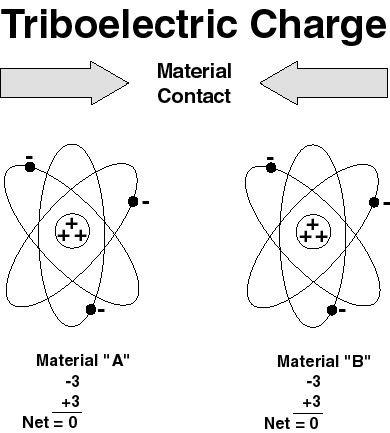
Creating electrostatic charge by contact and separation of materials is known as triboelectric charging. It involves the transfer of electrons between materials. The atoms of a material with no static charge have an equal number of positive (+) protons in the nucleus and negative (-) electrons orbiting the nucleus. In Figure 1, Material "A" consists of atoms with equal numbers of protons and electrons. Material B also consists of atoms with equal (though perhaps different) numbers of protons and electrons. Both materials are electrically neutral.

Figure 1: The Triboelectric Charge. Materials Make Intimate Contact
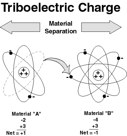
When the two materials are placed in contact and then separated, negatively charged electrons are transferred from the surface of one material to the surface of the other material. Which material loses electrons and which gains electrons will depend on the nature of the two materials. The material that loses electrons becomes positively charged, while the material that gains electrons is negatively charged. (Shown in Figure 2.)

Figure 2: The Triboelectric Charge - Separation
Static electricity is measured in coulombs. The charge (q) on an object is determined by the product of the capacitance of the object (C) and the voltage potential on the object (V):
q = CV
However, commonly we speak of the electrostatic potential on an object, which is expressed as voltage.
The process of material contact, electron transfer, and separation is a much more complex mechanism than described here. The amount of charge created by triboelectric generation is affected by the area of contact, the speed of separation, relative humidity, the chemistry of the materials, surface work function, and other factors. Once the charge is created on a material, it becomes an electrostatic charged material or object (if the charge remains on the material or object). This charge may be transferred from the material, creating an electrostatic discharge or ESD event. Additional factors, such as the resistance of the actual discharge circuit and the contact resistance at the interface between contacting surfaces, also affect the actual charge that is released. Typical charge generation scenarios and the resulting voltage levels are shown in Table 1. Also, the contribution of humidity to reducing charge accumulation is shown. However, it should be noted that static charge generation still occurs even at high relative humidity.
Table 1. Examples of Typical Static Generation Voltage Levels
|
Means of Generation Walking across carpet Walking across vinyl tile |
10-25% RH 35,000V 12,000V |
65-90% RH 1,500V 250V |
|
Worker at bench |
6,000V |
100V |
|
Polybag picked up from the bench |
20,000V |
1,200V |
|
Chair with urethane foam |
18,000V |
1,500V |
An electrostatic charge may also be created on the material in other ways, such as by induction, ion bombardment, or contact with another charged object. However, triboelectric charging is the most common.
HOW MATERIAL CHARACTERISTICS AFFECT STATIC CHARGE
Triboelectric Series
When two materials contact and separate, the polarity and magnitude of the charge are indicated by the materials' positions in a triboelectric series. The triboelectric series tables show how charges are generated on various materials. When two materials contact and separate, the one nearer the top of the series takes on a positive charge, the other a negative charge. Materials further apart on the table typically generate a higher charge than ones closer together. These tables, however, should only be used as a general guide because there are many variables involved that cannot be controlled well enough to ensure repeatability. A typical triboelectric series is shown in Table 2.
Table 2. Typical Triboelectric Series
|
+ Positive |
|
|
Negative - |
Rabbit fur |
Virtually all materials, including water and dirt particles in the air, can be triboelectrically charged. How much charge is generated, where that charge goes, and how quickly, are functions of the material's physical, chemical, and electrical characteristics.
Insulative Materials
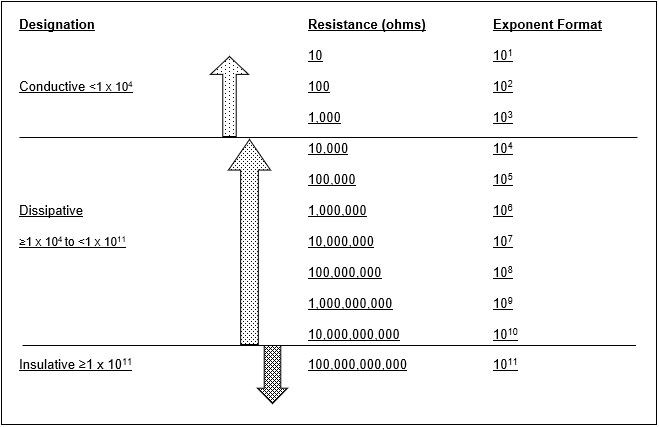
A material that prevents or limits the flow of electrons across its surface or through its volume, due to having an extremely high electrical resistance, is called an insulative material. ESD ADV1.0 defines insulative materials are defined as "materials with a surface resistance or a volume resistance equal to or greater than 1.0 × 10¹¹ ohms". A considerable amount of charge can be generated on the surface of an insulator. Since an insulative material does not readily allow the flow of electrons, both positive and negative charges can reside on an insulative surface at the same time, although at different locations. The excess electrons at the negatively charged spot might be sufficient to
satisfy the absence of electrons at the positively charged spot. However, electrons cannot easily flow across the insulative material's surface, and both charges may remain in place for a very long time.
Conductive Materials
A material that allows electrons to flow easily across its surface or through its volume is called a conductive material. ESD ADV1.0 defines conductive materials as "a material that has a surface resistance of less than 1.0 × 10⁴ ohms or volume resistance of less than 1.0 × 10⁴ ohms". When a conductive material becomes charged, the charge (the deficiency or excess of electrons) will be uniformly distributed across the surface of the material. If the charged conductive material makes contact with another conductive material, the electrons will be shared between the materials quite easily. If the second conductor is attached to AC equipment ground or any other grounding point, the electrons will flow to ground, and the excess charge on the conductor will be neutralized.
Electrostatic charge can be created triboelectrically on conductors the same way it is created on insulators. As long as the conductor is isolated from other conductors or ground, the static charge will remain on the conductor. If the conductor is grounded, the charge will easily go to ground. Or, if the charged conductor contacts another conductor of different electrical potential, the charge will flow between the two conductors.
Dissipative Materials
Dissipative materials have an electrical resistance between insulative and conductive materials. ESD ADV1.0 defines dissipative materials as "a material that has a surface resistance greater than or equal to 1.0 × 10⁴ ohms but less than 1.0 × 10¹¹ ohms or a volume resistance greater than or equal to 1.0 × 10⁴ ohms but less than 1.0 × 10¹¹ ohms. There can be electron flow across or through the dissipative material, but it is controlled by the surface resistance or volume resistance of the material.
As with the other two types of materials, a charge can be generated triboelectrically on static dissipative material. However, like the conductive material, the static dissipative material will allow the transfer of charge to ground or other conductive objects. The transfer of charge from a static dissipative material will generally take longer than from a conductive material of equivalent size. Charge transfers from static dissipative materials are significantly faster than from insulators and slower than from conductive material.

Figure 3: Resistance Classifications (from ANSI/ESD S541)
Electrostatic Fields
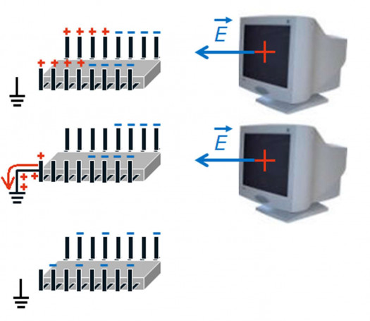
Charged materials also have an electrostatic field and lines of force associated with them. Conductive objects brought into the vicinity of this electric field will be polarized by a process known as induction. (See Figure 4.) A negative electric field will repel electrons on the surface of the conducting item that is exposed to the field. A positive electric field will attract electrons near the surface, thus leaving other areas positively charged. No change in the actual charge on the item will occur in polarization. However, if the item is conductive or dissipative, and is connected to ground while polarized, the charge will flow from or to ground due to the charge imbalance. If the ground contact is disconnected and then the electrostatic field is removed, the charge will remain on the item. If a nonconductive object is brought into the electric field, the electrical dipoles will tend to align with the field creating apparent surface charges. A nonconductor (insulative material) cannot be charged by induction.

Figure 4: Induction
ESD DAMAGE—HOW DEVICES FAIL
Per ESD ADV1.0, electrostatic damage is defined as "change to an item caused by an electrostatic discharge that makes it fail to meet one or more specified parameters". It can occur at any point, from manufacture to field service. Typically, damage results from handling the devices in uncontrolled surroundings or when poor ESD control practices are used. Generally, the damage is classified as either a catastrophic failure or a latent defect.
Catastrophic Failure
When an electronic device is exposed to an ESD event, it may no longer function. The ESD event may have caused a metal melt, junction breakdown, or oxide failure. The device's circuitry is permanently damaged, causing the device to stop functioning totally or at least partially. Such failures usually can be detected when the device is tested before shipment. If a damaging level ESD event occurs after testing, the part may go into production, and the damage will go undetected until the device fails in final testing.
Latent Failure
Per ESD ADV1.0, latent failure is "a malfunction that occurs following a period of normal operation. Note: The failure may be attributable to an earlier electrostatic discharge event. The concept of latent failure is controversial and not fully accepted by all in the technical
community". A device that is exposed to an ESD event may be partially degraded, yet continue to perform its intended function. Therefore a latent defect is difficult to identify. Still, the operating life of the device may be reduced. A product or system incorporating devices with latent defects may experience premature failure after the user places them in service. Such failures are usually costly to repair and, in some applications, may create personnel hazards.
With the proper equipment, it is relatively easy to confirm that a device has experienced a catastrophic failure as basic performance tests will substantiate device damage. However, latent defects are challenging to prove or detect using current technology, especially after the device is assembled into a finished product.
BASIC ESD EVENTS—WHAT CAUSES ELECTRONIC DEVICES TO FAIL?
ESD damage is usually caused by one of three events: direct ESD to the device, ESD from the device, or field-induced discharges. Whether or not damage occurs to an ESD susceptible item (ESDS) by an ESD event is determined by the device's ability to dissipate the energy of the discharge or withstand the voltage levels involved. The level at which a device fails is known as the device's ESD sensitivity or ESD susceptibility.
Discharge to the Device
An ESD event can occur when any charged conductor (including the human body) discharges to an item. A cause of electrostatic damage could be the direct transfer of electrostatic charge from the human body or a charged material to the ESDS. When a person walks across a floor, an electrostatic charge accumulates on their body. Simple contact (or proximity) of a finger to the leads of an ESDS or assembly, which is typically at a different electrical potential, can allow the body to discharge and possibly cause ESD damage to the ESDS. The model used to simulate this event is the human body model (HBM). A similar discharge can occur from a charged conductive object, such as a metallic tool or fixture. From the nature of the discharge, the model used to describe this event is known as the machine model (MM).
Discharge from the Device
The transfer of charge from an ESDS to a conductor is also an ESD event. Static charge may accumulate on the ESDS itself through handling or contact and separation with packaging materials, worksurfaces, or machine surfaces. This frequently occurs when a device moves across a surface or vibrates in a package. The model used to simulate the transfer of charge from an ESDS is referred to as the charged device model (CDM). The capacitances, energies, and current waveforms involved are different from those of a
discharge to the ESDS, likely resulting in different failure modes.
The trend towards automated assembly would seem to solve the problems of HBM ESD events. However, it has been shown that components may be more sensitive to damage when assembled by automated equipment. For example, a device may become charged
by sliding down the feeder. When it contacts the insertion head or any other conductive surface, a rapid discharge occurs from the device to the metal object.
Field-Induced Discharges
Another electrostatic charging process that can directly or indirectly damage devices is termed field induction. As noted earlier, whenever any object becomes electrostatically charged, there is an electrostatic field associated with that charge. If an ESDS is placed in the electrostatic field and grounded while located within the electrostatic field, a transfer of charge from the device occurs as a CDM event. If the item is removed from the region of the electrostatic field and grounded again, a second CDM event will occur as the charge (of opposite polarity from the first event) is transferred from the device.
HOW MUCH ESD CONTROL PROTECTION IS NEEDED?
Damage to an ESDS by an ESD event is determined by the device's ability to dissipate the energy of the discharge or withstand the voltage levels involved in the discharge. As explained previously, these factors determine the ESD sensitivity of the device. Test procedures based on the models of ESD events help define the sensitivity of components to ESD. Although it is known that there is very rarely a direct correlation between the discharges in the test procedures and real-world ESD events, defining the ESD sensitivity of electronic components gives some guidance in determining the degree of ESD control protection required. These procedures and more are covered in Part Five of this series.
Per ESD ADV1.0, the ESD withstand voltage is "the highest voltage level that does not cause device failure; the device passes all tested lower voltages". Many electronic components are susceptible to ESD damage at relatively low voltage levels. Many are susceptible at less than 100 volts, and many disk drive components withstand voltages even below 10 volts. Current trends in product design and development pack more circuitry onto these miniature devices, further increasing the sensitivity to ESD and making the potential problem even more acute. Table 3 indicates the ESD sensitivity of various types of components.
Table 3. ESD Sensitivity of Representative Electronic Devices or Parts with Sensitivity Associated with HBM and CDM*
|
Device or Part Type |
|
Microwave devices (Schottky barrier diodes, point contact diodes and other detector diodes >1 GHz) |
|
Discrete MOSFET devices |
|
Surface acoustic wave (SAW) devices |
|
Junction field-effect transistors (JFETs) |
|
Charged coupled devices (CCDs) |
|
Precision voltage regulator diodes (line of load voltage regulation, <0.5%) |
|
Operational amplifiers (OP AMPs) |
|
Thin-film resistors |
|
Integrated circuits |
|
GMR and new technology Disk Drive Recording Heads |
|
Laser Diodes |
|
Hybrids |
|
Very high-speed integrated circuits (VHSIC) |
|
Silicon controlled rectifiers (SCRs) with Io <0.175 amp at 10 °C ambient |
|
*Specific Sensitivity Levels are available from supplier data sheets |
SUMMARY
Part 1 of the ESD Fundamentals has discussed electrostatic charge and discharge, the mechanisms of creating a charge, materials, types of ESD damage, ESD events, and ESD sensitivity. We can summarize this discussion as follows:
- Virtually all materials, including conductors, can be triboelectrically
- The amount of charge is affected by material type, speed of contact and separation, humidity, and several other factors.
- Charged objects have electrostatic
- ESD can damage devices, so a parameter fails immediately, or ESD damage may be a latent defect that may escape immediate detection but may cause the device to fail prematurely.
- ESD can occur throughout the manufacturing, test, shipping, handling, or operational processes, and during field service
- ESD damage can occur as the result of a discharge to the device, from the device, or from charge transfers resulting from electrostatic fields. Devices vary significantly in their susceptibility to
Protecting products from the effects of ESD damage begins by understanding these fundamental concepts of electrostatic charges and discharges. An effective ESD control program requires an effective training program where all personnel involved understand the key concepts. See Part Two for the basic concepts of ESD control.
REFERENCES
ESD ADV 1.0, Glossary, EOS/ESD Association, Inc., Rome, NY.
ESD TR20.20, ESD Handbook, EOS/ESD Association, Inc., NY.
ESD ADV11.2, Triboelectric Charge Accumulation Testing, EOS/ESD Association, Inc., Rome, NY.
ANSI/ESD S20.20—Standard for the Development of Electrostatic Discharge Control Program, EOS/ESD Association, Inc., Rome, NY.