Small Form Factor CDM Testing: Part 1

Problems with FICDM Testing for Small Form Factor and Interface Die
ANSI/ESDA/JEDEC JS-002 [1] specifies how to test and qualify a product for a factory CDM event. The document is intended for the testing of packaged devices. Thus, CDM testers in the industry have mechanical stages and contact pins that are oriented towards products in packages with pin pitches typical of today’s package sizes. With shrinking footprints and increasing integration (for example, flip chip or wafer level chip scale packaging), bare die are being sold to original equipment manufacturers (OEMs). OEMs are asking the IC manufacturers to give a CDM rating for these packageless products. However, the existing CDM testers introduce issues when considering the testing of small form factor die. Additionally, there are products that have very low withstand voltages for CDM, and the traditional CDM testers do not produce reliable waveforms for voltages below 100V. This column discusses some of the issues with Field-Induced CDM (FICDM) testing, which is troublesome for small form factor and interface die.
The Need for Bare Die and Small Form Factor CDM Testing
Several industry segments are moving to packageless products. In the mobile phone industry, many products are now packageless. ICs have more integration on one chip, and the footprint continues to shrink. Antenna tuners and filters are sold directly to the OEMs as bare die for flip chip assembly. This is more attractive as there are cost savings, space savings and performance improvements in removing wire bonds.
The flip chip products pose problems for CDM testing. One problem is that the pitch of these bumps is so small that the pogo pin of an FICDM tester cannot contact one bump at a time. In addition, these die are small, which makes it difficult to hold the device in place on a FICDM tester.
Traditionally, multi-die packages have separate ICs inside the package. Therefore, the solder ball sizes and spacings were the same size and pitch as a package substrate. With the desire for increased connections between the different die in the package, manufacturers have developed a variety of 2.5D and 3D packaging solutions. Figure 1 illustrates a 3D IC stack.
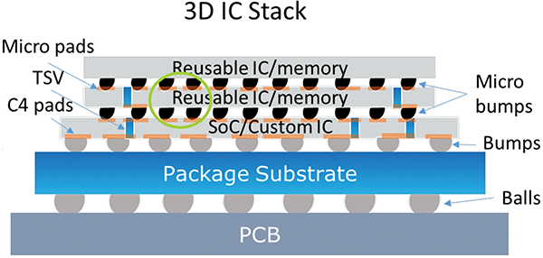 Figure 1: Die-to-die interface example, the green circle indicates a D2D interface
3D packaging uses a functional integrated circuit die on the bottom of a stack of two or more die, as shown in Figure 1. The base IC uses through substrate vias, TSV, to make connections between the upper die and the solder bumps on its bottom to accommodate connections to other ICs, often called chiplets. One of the most common applications for stacks of chiplets is memory. The manufacturing steps in 3D assembly provide multiple opportunities for CDM events, and the small size and pitch of the micro bumps present testing challenges.
Why FICDM is a Problem for Testing Bare Die
FICDM testing is an industry standard for gauging ESD susceptibility in manufacturing ICs. However, FICDM testing is frequently not suitable for testing small form factor die as listed here.
- FICDM testers may struggle to probe the small pads or bumps.
- The use of a modified pogo may change the ESD stress.
- Air discharge cannot be guaranteed at low voltages.
FICDM test results become unreliable at low voltages due to air discharge and contact impedance variability.
Probe Too Large for Die Bumps or Pads
Figure 2 shows a die with pads lined up near the edge. The radius of the probe is about 245 µm, but the pad size is about 50 µm x 50 µm. In this situation, contact with a single pad cannot be achieved.
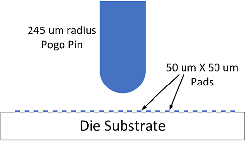 Figure 2: CDM tester probe radius and pad size photo and scale drawing
Package the Die
When a bare die product requires a CDM rating, mounting the die in a larger package and stressing the package may be an option. The purpose of the package is to allow the die to be tested on an FICDM tester without the arc terminating on the wrong pad. Analysis of the package must be performed to de-embed the response of the die from the die-in-package response. This process is difficult and time consuming. In addition, it is possible that false failures are induced because of the large amount of charge that the package will have as opposed to the bare die.
Testing Fine Pitch Die Bumps Using a FICDM Tester
Factors to consider with fine pitch are:
- A pointed pogo pin tip can change the nature of the arc due to the electric field enhancement at the sharp tip.
- The positional encoder and servomotor robotics of CDM testers may not be accurate enough to optimally position the pogo pin over the bump.
Peak Current Repeatability and Spark Impedance at Low Voltages
Below 250 volts, the air discharge spark becomes less repeatable as voltage drops because of the weaker electrical field and resultant weaker ionization of the air in the spark gap. The probability of getting the full discharge peak current appropriate for that voltage becomes lower. Also, as the voltage decreases, the variability of the spark length and the resistance of the plasma channel increase, causing the resistance of the spark to change. Die-to-die discharge can also occur without a spark gap when the voltage difference is below tens of volts. In this case, there is no additional spark channel resistance or inductance along the discharge path. This can have unpredictable effects on the peak current and rise time. Variations in rise time and pulse width can significantly affect the failure mechanisms created by an ESD event.
Summary
FICDM testers with a pogo pin are unsuitable for bare-die or interface die testing. First, the minimum pogo pin tip diameter is too large for testing microbumps used in small form factor products. Second, the variability of spark discharges at voltages below 250 volts is not predictable. Packaging a die for testing with the FICDM tester is also possible. This method delivers the quickest results because it uses common FICDM testers. However, the package’s complex post-test de-embedding is required to deliver correct die-level results.
There exist several viable options for bare-die CDM testing. There is no consensus on which one of these options is the best. The follow-on papers to this introduction will review what has been used in the industry, along with the pros and cons of each approach.
Acknowledgements
This three-part publication is part of a summary of a technical report published by the ESD Association. We would like to acknowledge the authors of the technical report:
- Robert Ashton (retired)
- David Epps (AMD)
- Jared Floyd (ESDEMC)
- Wei Huang (ESDEMC)
- David Klien (pSemi)
- Tom Meuse (Thermo Fisher)
- Kathleen Muhonen (Qorvo)
- Friedrich sur Nieden (Infineon)
- Paul Phillips (Phasix)
- Michael Reardon (ESDEMC)
- Masnori Sawada (Hanwa)
- Jasmine Shen (ESDEMC)
- Marko Simicic (IMEC)
- Heinrich Wolf (Fraunhofer)
Reference
- ANSI/ESDA/JEDEC JS-002, Charged Device Model (CDM) – Device Level, EOS/ESD Association.