Addressing an Industry Concern: The Demand for a CDM Bare Die Testing Method

Addressing an Industry Concern: The Demand for a CDM Bare Die Testing Method
Lena Zeitlhoefler, Theresa Lutz, Friedrich zur Nieden, Kai Esmark, Reinhold Gaertner, Infineon Technologies AG, on behalf of EOS/ESD Associaiton, Inc.
Background
The definition and verification of CDM targets for single dies in 2.5D or 3D devices concerns the industry. Even if bare dies offer a low capacitance, recent studies have shown that significant discharge current levels can be reached during a CDM-like discharge, e.g., at a very low charging voltage of 5 V, 500 mA can be reached [1]. The question of whether existing CDM targets should be scaled down for bare dies to accommodate lower charging voltages is raised [2].
Testing of single bare dies using the Field‐Induced CDM (FICDM) setup acc. to JS002 [3] standard is not possible. One issue is the difficulty of touching bare die pads with the pogo‐pin, whose diameter can exceed the pad size. Moreover, FICDM testing at voltages below 20 V leads to unstable waveforms. The standardized testing setup does not reflect the real capacitance and peak current relationship due to the small dimensions and thickness of the dies, which affect CDM peak currents, rise times, and pulse widths. There are arguments for using alternative testing methods, such as CCTLP, to enable the testing of bare dies [4].
These challenges are addressed by an alternative approach that transforms CDM charging voltage into current using the parameter device volume and effective capacitance Ceff. This transformation [5] facilitates alternative testing methods like Capacitively Coupled Transmission Line Pulsing (CCTLP). The capacitance is proportional to the product dimensions. Besides the area, the thickness of a die influences the peak current.
Capacitance and Volume
CDM voltage can be translated into a CCTLP current level based on the capacitance and volume of the product [5]. 3D-Simulations with idealized metallic cuboids of various dimensions demonstrate that Ceff is directly proportional to the area, showing saturation as cuboids increase in size.
Figure 1 shows the relation between device dimensions in volume versus the Ceff in a CDM tester. The solid lines represent the upper limit for a device dimension coming from the static capacitance simulation with fully metallic cuboids. The products always lay below the solid line, and the respective height is color-coded. The simulation shows that height itself has only an influence if the height itself surpasses the side length of the fully metallic body. For packaged devices, the experiments show a contrary effect in a way that the capacitance decreases with height. This is because the slimmer the packages, the more percentage of conductive material they include that contributes to the device capacitance.
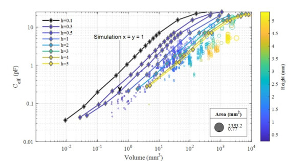
Figure 1. Simulated cuboid values with varying square base dimensions and heights (solid line) in comparison to calculated effective capacitance from the product’s current waveform integral extracted from the database. The red and green markers refer to the dimensions of the test devices in the standard CDM setup and a CDM setup with a tenfold reduced dielectric thickness.
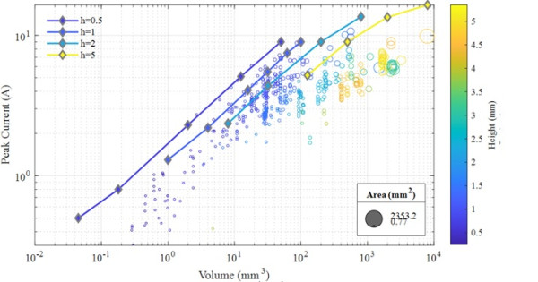
Figure 2. Comparison of upper limit for peak current of fully metallic cuboids in comparison to measured data for real products. Datasets focus on different values for the height of the package/cuboid from 0.5 mm and 5 mm.
Peak Current and Volume
Figure 2 shows the maximum measured peak current at 500 V respective to its volume. It compares actual measurement results from products and simulation data from cuboids with varying square base dimensions from 0.3 mm to 60 mm x/y length and varied heights. The peak currents for real products always stay below their theoretical limit defined by the cuboids, making this a valuable worst-case estimation. The gap between the limit and real data is much smaller for slim packages than for packages with increased height. In some cases, the gap almost vanishes. The reason is that the “conductive” share of the package volume of slim packages (especially chip scale packages) comes very close to the volume of metallic cuboids.
Bare dies are not incorporated in any package, and, therefore, deliver the largest Ceff values according to
their body dimensions. The maximum peak current relative to their dimensions can be achieved for bare dies without packaging, highlighting the importance of a current-based target level. This can be deduced from Figure 3 for different packaged devices.
Conclusion
Waveforms for bare dies at low charging voltage of, e.g., 20 V, are very fast and can hardly be measured. The importance of such pulse parameters for device failure has been shown in [7] and [8]. In Figure 4, CCTLP waveforms of a bare die (2x2 mm2) referring to a CDM voltage of 20 V are shown. The measured CDM curves vary between 10 mA and 30 mA. The waveforms are presented for a 30 ps rise time.
The increasing prevalence of products with stacked dies necessitates defining and verifying design targets at low charging voltage levels. Current CDM testing methods, specifically the FICDM tester, are inadequate for bare dies due to issues with contact and reproducibility. CCTLP, however, offers a method with reliable and stable testing even for low charging voltages leading to currents in the mA range.
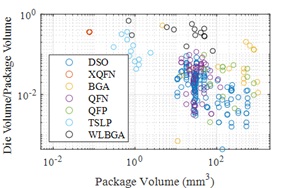
Figure 3. Volume of the die relative to the package volume for certain package types
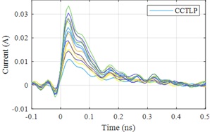
Figure 4. CCTLP waveforms of a bare die with size 2x2 mm. The current refers to a 20 V CDM charging voltage.
References
- Johnsson, P. Tamminen, T. Viheriäkoski and H. Gossner, "Discharge Waveforms of Emulated Die-to-Die ESD Discharges," 2023 45th Annual EOS/ESD Symposium (EOS/ESD), Riverside, CA, USA, 2023, pp. 1-9
- Fellner, D. Pommerenke, L. Zeitlhoefler, F. zur Nieden, " Transmission Line Based CDM ESD Current Target to Overcome Bandwidth Limitations," International Symposium and Exhibition on Electromagnetic Compatibility EMC Europe 2024, Bruges, Belgium, 2024.
- ANSI/JEDEC/ESDA, “Joint Standard for Electrostatic Discharge Sensitivity Testing – Charged Device Model,” JS-002, 2018.
- ANSI/ESD, Standard Practice for Electrostatic Discharge Sensitivity Testing – Charged Device Model (CDM) Testing – Component Level – Capacitively Coupled – Transmission Line Pulsing as an Alternative CDM Characterization Method, SP5.3.4-2022
- Zeitlhoefler, T. Lutz, F. Zur Nieden, K. Esmark and R. Gaertner, "Voltage to Current Correlation for CDM Testing," 2023 45th Annual EOS/ESD Symposium (EOS/ESD), Riverside, CA, USA, 2023, pp. 1-11.
- Johnson, R. Ashton and S. Ward, "FCDM measurements of small devices," 2009 31st EOS/ESD Symposium, Anaheim, CA, USA, 2009, pp. 1-8.
- Zeitlhoefler, F. Z. Nieden, K. Esmark and R. Gaertner, "Limitation of CDM Testing for Small Devices," 2022 44th Annual EOS/ESD Symposium (EOS/ESD), Reno, NV, USA, 2022, pp. 1-9
- Eichenseer, G. Langguth, R. Gaertner, F. Z. Nieden, L. Zeitlhoefler and S. Kokorovic, "Fast Transient ESD Protection at RF Pins," 2023 45th Annual EOS/ESD Symposium (EOS/ESD), Riverside, CA, USA, 2023,