In-situ ESD Current Sensing in a Pick-and-Place Machine

In the rapidly evolving semiconductor industry, the shift towards Multi-Chip Modules (MCM) and Systems in a Package (SiP) is notable. These advanced assemblies comprise multiple chiplets, sensors, and optoelectronic components, which are vulnerable to Electrostatic Discharge (ESD). The complex internal architecture of MCMs and SiPs—with their internal pins and through-silicon vias—poses challenges for ESD protection in assembly processes.
During the assembly of these systems, components may be exposed to ESD stress. Established methods for assessing the Charged Device Model (CDM) [1] robustness of individual devices exist, including advanced methods such as Capacitively-Coupled Transmission Line Pulsing (CC-TLP) [2]-[7] or low-impedance contact CDM (LICCDM) [8] [9]. While CC-TLP yields reproducible results even for bare dies or wafers, it uses current to determine the robustness level. Insufficient data currently exists regarding the correlation between charging voltages in production machines and discharge currents during the assembly process. This study proposes a method to measure discharge currents during the pick and place process, aiming to link this current to a pre-charge voltage and enhance the evaluation of ESD protection requirements for internal pins.
The Discharge Current Sensor
By employing a dedicated Discharge Current Sensor (DCS), it is possible to gather real-time data on discharge currents, providing insights into the maximum currents that need consideration during the design phase of ESD protection schemes.
The DCS (Figure 1) developed for this study is a compact setup designed for integration within assembly machines. It utilizes a 50 Ω microstrip line (2) terminated by a miniature pogo-pin (3). Using up to 10 thin-film resistors between the pogo-pin and ground plane, it allows to accurately measure the discharge current. The sensor’s design allows for minimal mismatch and high-frequency bandwidth.
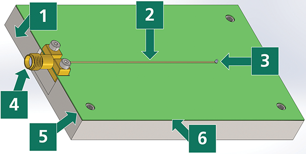 Figure 1: Discharge current sensor
Insights from Laboratory Measurements
Initial laboratory measurements using the DCS focused on three different die sizes and various pre-charge voltage levels. The DCS was placed below the pick-and-place head with the miniature pogo-pin facing the DUT (Figure 2). The DUT was charged with the charging probe and finally discharged via the pogo-pin into a microstrip line connected to a high bandwidth oscilloscope.
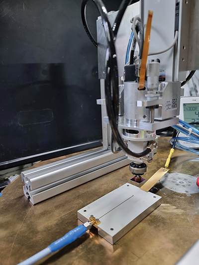 Figure 2: Measurement setup in laboratory
The laboratory experiments showed some first statistical data on discharge currents for voltage levels ranging between 4 V and 100 V (Figure 3) highlights the measured peak currents for pre-charge voltages < 30 V). Interestingly, the tests revealed that discharge currents were lower than anticipated compared to interpolated CDM values. Furthermore, the measured discharge currents displayed faster rise times (< 50 ps) and shorter pulse widths (< 100 ps). These findings emphasize the importance of real-world measurements in understanding ESD risks during assembly processes, suggesting that the current protection schemes may need re-evaluation to better align with actual industrial conditions.
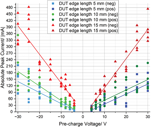 Figure 3: Measured peak currents for pre-charge voltages <30 V
Real-World Application: In-Situ Measurements
The research progressed to in-situ measurements within a state-of-the-art pick-and-place machine. An isolated picking tool and fully metallized dies were employed to emulate the worst-case scenario. The tests consisted of picking a die (edge length 10 mm) from a blue tape carrier and placing it on the pogo-pin of the DCS. These tests illustrated that factors such as tool speed and the time between picking and placing of components significantly affect the discharge currents.
For instance, as tool speed increased, so did the discharge current, highlighting the need for careful control of assembly parameters to mitigate ESD risks (Figure 4). Additionally, the path taken by the picking tool—whether directly to the sensor or via an alignment camera—also significantly influenced the peak discharge current.
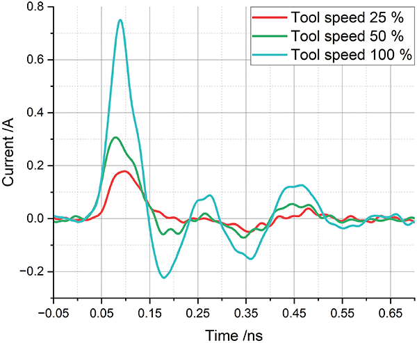 Figure 4: Dependency of the measured current on the tool speed
Conclusion and Future Directions
This research introduced a DCS designed for in‑situ ESD measurements in assembly machines. Laboratory experiments established a link between voltage levels and measured discharge currents, providing initial statistical data across three different device sizes. Notably, the discharge curves observed do not align with extrapolated data of the JS-002 standard, exhibiting lower peak currents, faster rise times, and shorter pulse widths. Additionally, tests in a pick-and-place machine reveal higher ESD risks associated with increased tool speeds and reduced intervals between charging and discharging the die. The sensor serves as a valuable tool for verifying and enhancing production machines, offering insights into assembly process risks that can help MCM and SiP designers in optimizing ESD protection tailored to specific needs.
Looking ahead, further statistical data collection is essential, necessitating the development of an automated measurement setup. Efforts are already underway to create a redesigned DCS that will allow high-volume measurements.
References
- ESDA/JEDEC Joint Standard ANSI/ESDA/JEDEC JS-002-2022 Charged Device Model (CDM) – Device Level.
- ANSI/ESD SP5.3.4-2022, ESD Association Standard Practice for Electrostatic Discharge Sensitivity Testing – Charged Device Model (CDM) Testing – Component Level – Capacitively Coupled – Transmission Line Pulsing as an Alternative CDM Characterization Method.
- H. Wolf, H. Gieser, W. Stadler, W. Wilkening, “Capacitively Coupled Transmission Line Pulsing CC-TLP – A Traceable and Reproducible Stress Method in the CDM-Domain,” Journal of Microelectronics Reliability, Elsevier, Vol. 45, No. 2, 2005, pp. 279-285.
- H. Wolf, H. Gieser, K. Bock, A. Jahanzeb, C. Duvvury, and Y.-Y. Lin, “Capacitive coupled TLP (CC-TLP) and the correlation with the CDM,” 2009 31st Annual EOS/ESD Symposium, Anaheim, CA, USA, 2009.
- K. Esmark, R. Gärtner, S. Seidl, F. zur Nieden, H. Wolf, H. Gieser, “Using CC-TLP to get a CDM Robustness Value”, 2015 37th Annual EOS/ESD Symposium (EOS/ESD), Reno, NV, USA, 2015.
- J. Weber, K. T. Kaschani, H. A. Gieser, H. Wolf, L. Maurer, N. Famulok, R. Moser, K. Rajagopal, M. Sellmayer, A. Sharma, and H. Tamm, “Correlation study of different CDM testers and CC-TLP,” 2017 39th Annual EOS/ESD Symposium, Tucson, AZ, USA.
- J. Weber, R. Fung, R. Wong, H. Wolf, H. A. Gieser, L. Maurer, “Stress current slew rate sensitivity of an ultra-high-speed interface IC,” IEEE Transactions on Device and Materials Reliability, Vol. 19, Issue 4, November 2019.
- N. Jack, B. Carn, and J. Morris, “Toward Standardization of Low Impedance Contact CDM,” 2019 41st Annual EOS/ESD Symposium, Riverside, CA, USA, 2019.
- M. Simicic, W.-M. Wu, N. Jack, S. Tamura, Y. Shimada, M. Sawada, S.-H. Chen, “Optimization of Wafer-Level Low-Impedance Contact CDM Testers,” 2020 42nd Annual EOS/ESD Symposium, Reno, NV, USA, 2020.