How TVS Properties and Printed Circuit Board Design Influence Peak Voltage and Residual Current At An IC For USB-C Superspeed Data Lines

How TVS Properties and Printed Circuit Board Design Influence Peak Voltage and Residual Current At An IC For USB-C Superspeed Data Lines
Steffen Holland, Nima Lotfi, Martin Pilaski, Burkhard Laue, Stefan Seider, Nexperia Germany GmbH, on behalf of EOS/ESD Association, Inc.
The new connector standard USB-C includes both power delivery of currently up to 20 V as well as SuperSpeed data lines. ICs receiving signals on these data lines are very ESD sensitive. The Vbus pins in the USB-C connector are placed directly next to the SuperSpeed Tx and Rx pins which poses the risk that the data pins can temporarily short to the supply voltage. The USB-C specification requires a mandatory AC coupling capacitor placed on the data lines in front of the IC when USB4 is used on the SuperSpeed lines. Thus, TVS devices for system level protection can be placed either behind the AC coupling capacitor or in front of it.
In this article the effect of the TVS placement and the device properties on the IC is investigated. Special PCBs have been produced; one is shown in Figure 1. The distance between TVS and an IC replacement consisting of a 2 Ohm resistor and a forward biased diode is varied. The voltage at the IC can be measured. The IC residual current is determined by measuring the voltage drop across the resistor. Six different TVS protection devices have been chosen. All of them have a capacitance of less than 0.2 pF which makes them suitable for the SuperSpeed application. Two of them are placed in front of the capacitor. However, to avoid turning on during a short to the power line these TVS device requires a breakdown voltage larger than 20V. For a placement behind the capacitor a high breakdown voltage is not needed. An overview of the TVS parameters is shown in Table 1.
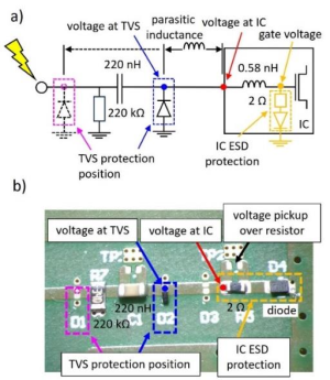
Figure 1: a) schematic representation of the application. b) real populated board with the smallest trace length distance between TVS and IC ESD replacement.
Table 1: Overview of electrical parameters of chosen TVS devices.
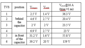
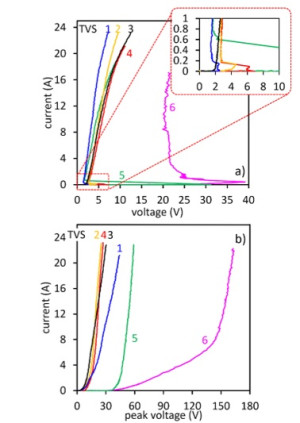
Figure 2: a) Quasi-static TLP curves of the TVS devices. The inset shows the curves at low currents b) Peak voltage of the components obtained by Very-Fast-TLP measurements.
Transmission Line Pulse (TLP) and Very-Fast-TLP measurements of the TVS devices have been performed with a rise time of 1 ns. The results are shown in Figure 2.
The Devices are chosen such that the different parameters have a wide range of values. TVS 1 to 4 have different trigger, peak and holding voltages. A comparison allows to investigate the effect on the maximum input voltage and residual current into the IC. TVS 5 and 6 both have breakdown and trigger voltages larger than 20 V. The difference is that TVS 5 is a deep snapback device while TVS 6 does not snap back to below 20 V for all currents.
Figure 3 a) shows the residual current into the IC and b) the peak voltage at the IC. While TVS 5 can strongly reduce the IC current after turning on, TVS 6 manages to divert only about 50% away from the IC. This is a
direct effect of its high holding voltage. TVS 6 also exhibits a high peak voltage which leads to a high peak IC input voltage. Even when the device turns on at 14 A, the peak IC input voltage is barely clamped. TVS 5 can limit the peak IC input voltage much more effectively. However, in comparison to the TVS 1 to 4 with their much lower trigger voltages the absolute value is still higher. Compared to TVS 2 with the lowest peak IC input voltage the value is 50% higher at 16 A. One can conclude that TVS devices with high trigger voltage which can be placed in front of the AC coupling capacitor would in principle be able to protect the capacitor. However, they are ill-suited for an effective system level ESD protection of sensitive SuperSpeed ICs.
Surprisingly, for the trigger voltage range of TVS 1 to 4 the trigger voltage value has only a small effect on the peak IC input voltage. At high currents it correlates with the peak voltage of the TVS device.
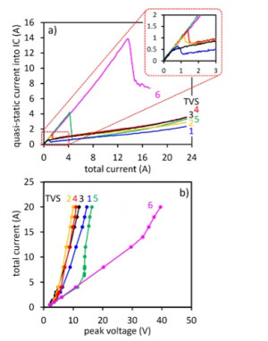
Figure 3: a) Residual current into the IC. The inset is a magnification of the low current range. b) Peak voltage at the IC input.
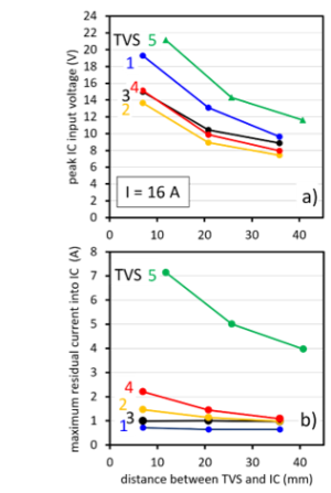
Figure 4: a) Peak IC input voltage and b) maximum residual current into the IC for different trace lengths.
Figure 4: a) Peak IC input voltage and b) maximum residual current into the IC for different trace lengths.
Figure 4 shows that a longer trace length between TVS protection and the IC replacement can significantly reduce the peak voltage at the IC as well as the maximum residual current into it.
In conclusion, placing a TVS protection in front of the AC-capacitor does not offer a good IC protection. Low peak voltages at the IC can be achieved by lowering the peak voltage of the TVS protection and increasing the PCB trace length. The maximum residual current can be limited by reducing the trigger voltage of the TVS protection.
Reference
[1] S. Holland, N. Lotfi, M. Pilaski, B. Laue and S. Seider, "Influence of TVS Properties and Printed Circuit Board Design on System Level ESD Robustness for USB-C SuperSpeed data lines," 2024 46th Annual EOS/ESD Symposium (EOS/ESD), Reno, NV, USA, 2024, pp. 1-10, doi: 10.23919/EOS/ESD61719.2024.10702133.